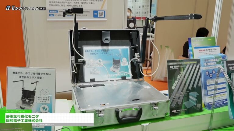

Exhibition Description
Materials, components, and manufacturing equipment technology for semiconductor post-processing, semiconductor manufacturing technology, chiplets (2.5D/3D packaging), advanced chiplet technology, semiconductor post-processing technologies, TSV (through-silicon via) and RDL (redistribution layer), packaging technology, materials, and components, heterogeneous bonding, sealing materials, resists, other materials and components, package substrates (printed circuit boards, tape substrates, ceramic substrates), package analysis and simulation software, grinding, dicing, die bonding, wire bonding, molding technologies, materials, equipment, and products, analytical equipment, inspection equipment, universities and research institutes
Semiconductor back-end processing technology is becoming increasingly diverse as an important area for realizing higher performance, smaller size, lower power consumption, and improved reliability of devices while responding to evolving market needs. In recent years, 3D packaging technology, chiplet technology, and the use of advanced materials have attracted attention, opening up new possibilities that go beyond conventional technologies. Against this background, we have launched a new exhibition, "SEMISOL - Semiconductor Post-Processing Technology & Solutions Expo," focusing on adding high added-value to post-processing that supports the evolution of the semiconductor industry. This exhibition will provide a forum for promoting the development of the industry with the theme of markets and innovative technologies and solutions that support the next generation, such as AI, 5G, IoT, and automotive applications.
Held with a concurrent exhibition.